
A Gerber története
More than 95% of all PCB designs produced worldwide are transferred from designer to fabricator as Gerber files. On most CAD systems the Gerber files are output automatically. It is only rarely the designers have to concern themselves about how a Gerber file represents their data. This in itself is a good measure of the power and ubiquity of the format, but occasionally an issue arises where some background knowledge may be helpful – and there are developments being planned for the format which will make it even more useful in future.
Gerber past:
Why “Gerber”?
Joe Gerber (1924 – 1996) was a US inventor who had fled from Austria to the US in 1940. Right from his student days he was interested in accurate data plotting, and during the 1950’s he developed the digital XY co-ordinate table which became the core of his future business, Gerber Scientific. The first product he launched using the new table was one of the world’s first digital drafting machines. Among later products was automatic cloth cutting machinery which is still widely used in the world’s garment industry. In the ‘80s he developed computerised equipment for machining spectacle lenses, again still used today.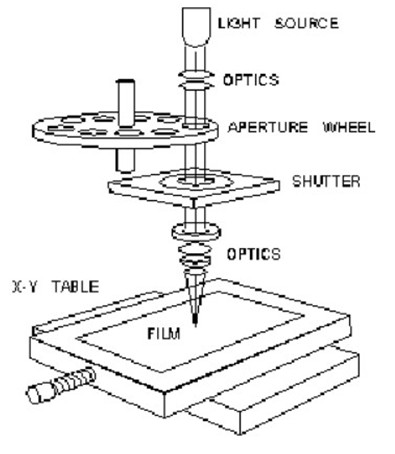
In the 1960s Joe Gerber found another use for his XY table. He introduced the world’s first NC photoplotter to generate the phototools used to produce PCBs. It worked by first moving an optical head containing a light source to the correct location over the film on the bed of the plotter. A circular wheel with different sized/shaped holes in it (apertures) was then rotated so that the correct aperture was under the light source. For a pad the light-source was flashed on and off, exposing the pad on the film. For a track the light was left on while the head moved, drawing the track on the film. Hence we still talk about “aperture tables”, and, less often these days, “flashes” and “draws”. The plotters were known as vector plotters as the head followed the actual pattern of the PCB. The actual drive format was based on a pre-existing format, RS-274-D, developed by the US Electronic Industries Association (EIA) to drive any NC machine. The data was loaded into the very first Gerber photoplotters on punched cards.
RS-274-D becomes RS 274X
By the early 1980s PCB Computer-Aided Design (CAD) systems were becoming more common, replacing the old hand-taped 2:1 artworks. CAD systems could output drive data directly to a photoplotter to generate the phototools. At that time most photoplotters were Gerber plotters. Other vendors moved into the photoplotter market, but as Gerber had published a full specification of their format in 1980, Gerber RS-274-D became the de facto standard.
As a vehicle for transferring PCB layer images, the format had one critical limitation: the size, shape and number of the apertures was limited by the physical aperture wheel. This worked (more or less) for designs using conventional through-hole components with round or square pads, but it couldn’t handle the new surface-mount components which used a wide variety of mainly rectangular pad sizes. Using RS-274-D the only solution was to “paint” the pads with tiny draws. Similarly, a simple plane layer could be plotted in reverse, that is, the clearance holes in the plane are plotted black and the board manufacturer reverses the polarity either in his front-end CAM system or physically by contact printing. But this won’t work for mixed plane layers or planes on signal layers. These had to be filled with draws. A large image with SMDs and planes could take up to 24 hours to plot on this type of plotter.
The solution was a new type of photo-plotter and a new format. The raster photo-plotter used a light source, typically a laser, to raster-scan the film in a continuous pattern. The image was built up by a sequence of laser on, laser off commands. Now any shape could be plotted, built up of raster pixels. Today this is the standard industry tool for photo-imaging PCBs, with laser photo-plotters using up to 48 independently-switched simultaneous beams plotting at resolutions down to 50,000 dots per inch or more.
Now it was possible to make the Gerber format more flexible and more suited to the requirements of the PCB designer. RS-274X or Extended Gerber was launched in 1991. This allowed the user to define and image any shape, as a pad, a track or a polygon (plane). The aperture definitions no longer depended on a physical wheel and so they could be derived automatically from the CAD job and included in the file as part of the output.
Gerber today.
RS-274X is the standard PCB layer image data transfer format used today. It is clear, unambiguous, and, if any questions arise, man-readable. Each file is complete and allows you to draw any pad-shape or copper area that you want.
The old Standard Gerber RS-274-D still lingers on, despite its drawbacks. It is very limited; it needs a separate aperture table which often seems to go missing; it produces huge and unwieldy files; the output may require the merging of positive and negative images which at best requires extensive clean-up and at worst generates hard-to-spot errors.
Eurocircuits can still accept the older format if needed, e.g. for old jobs, though it does not work with PCB Visualizer. However, Extended Gerber, RS-274X is our preferred format as it has none of the limitations of RS-274-D and as each file is complete including the embedded aperture definition it works with PCB Visualizer, offering you all the benefits of our advanced data checking technology. All current generation and most older CAD systems generate RS-274X output. If your CAD system is still outputting the old-style Gerber RS-274-D, look into the output settings. Sometimes it is possible to switch from RS-274-D to RS-274X. There may be different terminology used on different systems. If you are in doubt, ask us.
For more advice on input formats, go to our PCB Design Guidelines
Gerber tomorrow.
Extended Gerber, RS-274X, provides an exact and unambiguous image of the layers of a PCB, but there is still some layer information which is necessary for fabrication (especially for automated data preparation) but is not included in the format.
Examples include:
- What is the function of this layer: top copper, top solder mask, etc.?
- Does the image show a single PCB or a delivery panel?
- What is the function of this object: is it a SMD pad or a via pad, fiducial etc.?
- What is the board profile? Automatic recognition software like PCB Visualizer can recognize rectangular profiles but not complex shapes.
- What are the drill tolerances on this hole? For example, it may be a press-fit hole.
- Which are the impedance-controlled tracks?
- Which vias need to be filled?
The next step is to incorporate this type of information into the data transfer format. Any such further extension of the format has to be compatible with the existing format and with existing CAD systems. Although other formats have been proposed which can include non-image information, Gerber is so widely used and so effective in operation, that, like the QWERTY, QWERTZ and AZERTY keyboards, it cannot be easily replaced.
The Gerber format today is maintained and developed by the Belgian company Ucamco which bought the PCB Division of Gerber Scientific in 1997. Ucamco have recently published the blueprint for the next generation of RS-274X, Gerber RS-274X2. This adds attributes into the format which convey the information listed above.
This new development is further explained in our technical blog on Gerber X2. Eurocircuits are working closely with Ucamco on the new format as part of their drive to provide better tools for the European and global PCB design community. As the new attributes are implemented into CAD systems, we will add new functionality into our data input and validation procedures to handle them. Of course, we will also continue to accept the older Gerber formats.
Bővített Gerber – Gerber X2
Gerber”s new attributes set to transform CAD to CAM communication
With the support of Eurocircuits,, LPKF and AT&S, Ucamco drafted a new specification for a ground-breaking second extension to the Gerber format. This offers an unequivocal standard for non-image data that is just as simple, practical and universally accessible as the well-known Gerber image data format it now supports.
Ucamco“s Managing Director Karel Tavernier comments: “CAD/CAM professionals need to transmit data in a robust, reliable and cost-effective way, something the Gerber image format has been doing for years. It”s freely available, simple and to the point. It can be used by everybody, no matter how big or small the CAD or CAM operation is. It”s the most practical image description format out there, and by far the most used by our industry – every single day thousands of perfect PCB layer images are reliably transferred all over the world thanks to Gerber”.
Indeed, with Gerber, CAD/CAM professionals know that the most critical and fragile part of their archives – the image data – is secure and accurate. But there is another part of the PCB design that images cannot convey. This non-image data includes information about layer order and function, the differentiation between objects like SMD and via pads, and a raft of further information that, together with the image data, helps to translate designers” intentions into high performance products.
The problem is that there is currently no Gerber standard for transferring non-image data, leaving designers to decide for themselves how best to communicate with their manufacturing partners. They might add text files or drawings to their Gerber archive, or they might not, putting the onus on CAM engineers to search for the necessary information, or contact the designer if it”s missing. These are error-prone, time-consuming tasks that can end up affecting quality and deadlines, which can translate disastrously into loss of orders, clients and future business, especially in the time-critical context of prototypes and quick-turn boards. Thus whether you are a designer, customer or manufacturer of PCBs, data quality and clarity should be a top priority for you.
 This is why Ucamco has developed its Gerber X2 format. X2 offers a series of attributes that provide a standard for describing non-image data – some might rather grandly say that they add intelligence to the image data. Applicable either to a whole file or to individual graphic objects, Gerber”s standard attributes can now be used to define
- Gerber file function: top copper layer, top solder mask, etc.
- Part: single PCB, customer panel etc.
- Object function: SMD pad, via pad etc
- PCB profile
- Drill tolerances
- Locations of impedance-controlled tracks
- Filled vias
- An MD5 checksum for added security
The attributes have been purposely crafted, from scratch with the sole aim of supporting the transfer of PCB data from design to manufacturing. They are essential, simple and focused rather than a casual smorgasbord of “nice to haves” with unnecessary complexity, not to mention potential bugs. There is no overhead of manufacturing specific attributes as are found in CAM formats. X2 is simple and clean.
The attributes intentionally do not cover all possible non-image data. Ucamco refrained from adding the netlist to X2 as there is a simple and well-established format adequately describing netlists: IPC-356-A. Materials were not added as they are not linked to images and can be handled by a subset of IPC-2581 as soon as 2581 is opened up to partial implementations. In this way X2 delivers the best of all worlds: accessibility, simplicity, performance, and tried and tested formats that work for everybody. It”s a great combination that gives designers a clear and simple method for ensuring that their manufacturing partners have all the data necessary for efficient, reliable manufacture. And it eliminates the need to adopt complex new formats wholesale, which is a blessing, as Ucamco R&D engineer Thomas Weyn explains: “Imaging software, notoriously hard to implement, takes forever to debug and field test, especially for images as complex as PCBs. Here, errors are fiendishly difficult to detect and almost inevitably lead to scrap, so it is far preferable to keep what we know works (the Gerber image format) and support it, without disrupting it, with what is missing”.
A prime design goal of X2 is ease of adoption and of implementation. To fully exploit the productivity jump that X2 can bring, CAD and CAM software only requires quite minor updates. Given that the imaging model remains unchanged, it only requires adding a few extra lines with the attributes when writing a Gerber file – it could hardly be simpler. The payback for this is a more versatile product and greater competitivity for systems vendors. The attributes” use is not mandatory: they can be used wholesale, partially or not at all, whichever suits the implementation best. Most importantly, systems that have not been updated will still generate the correct image as Gerber X2 is upward compatible with previous versions of the format as the image is not affected by the attributes. Existing workflows are not broken by introducing X2.
Before the final version goes live, Ucamco encourages CAD and CAM professionals to look at it and in particular at the Attributes in Section 5, and participate in its fine-tuning by sending comments to gerber@ucamco.com
In order to make X2 happen, Ucamco need CAD software vendors to buy in to X2. As X2 is easy to implement, it makes a chance. But they need your support. Please write to Ucamco at gerber@ucamco.com and let them know that you support the Gerber X2 format, and that youy would implement it in your workflows when it is available.
The draft Gerber X2 second extension is available at www.ucamco.com/downloads and a brief press release describes the rationale for its development.
EUROCIRCUITS.TV – KIEMELT


![]()